- Home
- News Releases
- Back Issues
- June FY2025
- (Draft) OT Security Guidelines for Semiconductor Device Factories Compiled in Japanese and English Versions
(Draft) OT Security Guidelines for Semiconductor Device Factories Compiled in Japanese and English Versions
June 27, 2025
The Ministry of Economy, Trade and Industry (METI) has compiled the (Draft) OT Security Guidelines for Semiconductor Device Factories. These are factory security measure guidelines for Japan’s semiconductor industry that are in line with various global security standards for the semiconductor industry. METI has begun a 60-day public comment period for both Japanese and English versions of the draft guidelines. Moving forward, METI plans to finalize the guidelines around this fall based on the feedback received during the public comment period. Additionally, METI will explore linking the security measure standards outlined in the guidelines to the requirements of its investment promotion-related policies for the semiconductor industry.
1. Background and purpose
Cyberattacks have become increasingly diverse and sophisticated, leading to attacks on various control systems with operational technology (OT), which result in damage such as halts to factory production. Additionally, there is an increasing risk that various confidential information for development (i.e., intellectual property) could be leaked through cyberattacks. Considering the economic and national security importance of the semiconductor industry, as well as the growing cyberthreats and risks we face today, it is imperative to promote security measures, including countermeasures against advanced cyberattacks.
On the international stage, the global semiconductor industry association SEMI has developed the E187/E188 Standards for semiconductor manufacturing equipment. Furthermore, the National Institute of Standards and Technology (NIST) is working on the development of a semiconductor manufacturing profile for its Cybersecurity Framework 2.0 (NIST CSF 2.0).
In Japan, METI formulated and published the Cyber/Physical Security Guidelines for Factory Systems in 2022, targeting generic assembly-type factories. However, the guidelines are not suitable for semiconductor factories, which are generally categorized as process automation (PA) type factories, characterized by large-scale operations and a high number of manufacturing devices that utilize general-purpose operating systems (OS).
In light of this awareness of the issues at hand, METI has convened the Semiconductor Industry Sub-Working Group under the Industrial Cybersecurity Study Group, chaired by Professor Ezaki from the University of Tokyo, since November 2024. These meetings have involved various domestic and international companies and organizations, including semiconductor device manufacturers and suppliers of semiconductor manufacturing equipment. The purpose of these discussions is to explore the optimal approaches to security measures for OT systems in Japan’s semiconductor device factories.
As a result of these discussions, we have compiled the outcomes into a draft document titled the (Draft) OT Security Guidelines for Semiconductor Device Factories, to serve as factory security measure guidelines for Japan’s semiconductor industry in line with various global security standards for the semiconductor industry.
Given that Japan’s semiconductor industry operates within the framework of an international supply chain, we aim to gather broad feedback from stakeholders both domestically and internationally. To this end, we will conduct a 60-day public comment period for both the Japanese and English versions of the draft guidelines starting today.
2. Overview of the Draft Guidelines
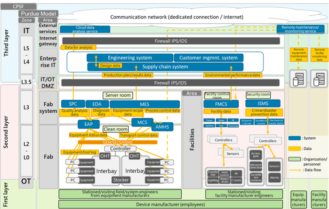
The draft guidelines are primarily intended for the manufacturing divisions of semiconductor device manufacturers, particularly at the practitioner level. The draft guidelines outline the necessary factory security measures to achieve an action level addressing the most sophisticated threats, such as advanced persistent threat (APT) groups supported by nation-states. The guidelines focus on safeguarding “Maintain Production Goals” (supply responsibilities), “Protect Confidential Information,” and “Maintain the Quality of Semiconductors". These security measure guidelines align with various security standards, including E187/E188 and NIST CSF 2.0.
The draft guidelines are expected to be utilized in the general process of advancing security measures in factories. For instance, they will be used during risk analyses that employ risk-based cybersecurity frameworks, such as the Cyber-Physical Security Framework (CPSF) and NIST CSF 2.0, which outline fundamental principles and specific guidelines for the integrative protection of cyberspace and physical space, as well as giving consideration to specific security measures.
The measures outlined in the draft guidelines can be broadly divided into the following two points.
- Security measures addressing risk sources (threats and vulnerabilities) specific to semiconductor device factories, identified by leveraging risk management frameworks (CPSF and NIST CSF 2.0) based on the reference architecture for semiconductor device factories.
- Measures for the following areas classified under the Purdue model: fab areas, fab system areas, external services, IT/OT DMZ (demilitarized zones between networks), and organizational/human aspects.
3. Outline of Public Comments
Subject of public comments
- (Draft) OT Security Guidelines for Semiconductor Device Factories: Japanese version
- (Draft) OT Security Guidelines for Semiconductor Device Factories: English version
Access to the materials
- Available on the METI website (refer to the “Related Materials” section on this page)
- Or available on the e-Gov portal, the comprehensive website for electronic government services
Due date
Submissions must be made between Friday, June 27, 2025, and the deadline of Tuesday, August 26, 2025 (Japan Standard Time, UTC+0900).
Submission of comments
Please proceed to the comment submission form available via the e-Gov portal (Note: instructions are provided in Japanese only) and submit your comments in either Japanese or English.
If accessing the e-Gov portal is difficult, you may complete the comment submission form provided in the attached document in either Japanese or English and send it via email to the address below.
- Please complete the “Attached Document: Comment Submission Form” found in the “Outline of Public Opinion” in either Japanese or English and send it to the email address below.
(Please send your e-mail with the subject line “Comments on the (Draft) OT Security Guidelines for Semiconductor Device Factories” and attach the comment submission form.) Note: Please be aware that we cannot accept comments submitted via telephone.
Notes:
The comments received will be used as a reference for making final decisions. However, please note that individual responses to submitted comments will not be provided. We appreciate your understanding in advance.
Please note that the submitted comments may be made publicly available, excluding personal information such as names, one numbers, fax numbers, and email addresses. However, if the submitted comments include personal information that could identify specific individuals or contain descriptions that may harm the property rights or other rights of individuals, corporations, or other entities, those portions will be redacted before publication.
Any personal information provided with your comments, such as names and contact details, will be managed appropriately and used solely for the purpose of contacting or clarifying unclear points regarding the submitted comments as part of this public consultation process.
4. Future Outlook
Moving forward, METI plans to finalize the guidelines around this fall based on the feedback received during the public comment period. Additionally, METI will explore linking the security measure standards outlined in the guidelines to the requirements of its investment promotion-related policies for the semiconductor industry.
Related Materials
The Robot Revolution & Industrial IoT Initiative (RRI) serves as the secretariat for the RING Project. Please refer to the RRI’s website if you are interested in our initiatives for local municipalities, support organizations, several groups, and private companies.
- Outline of Public Opinion(PDF:110KB)

- Summary of “(Draft) OT Security Guidelines for Semiconductor Device Factories”: English Version

- (Draft) OT Security Guidelines for Semiconductor Device Factories: English Version
Related Links
- Industrial Cybersecurity Study Group Working Group 1: Semiconductor Industry Sub-Working Group (in Japanese)
- Cyber/Physical Security Framework (CPSF) and its Deployment (in Japanese)
Divisions in Charge
Cybersecurity Division, Commerce and Information Policy Bureau
IT Industry Division, Commerce and Information Policy Bureau